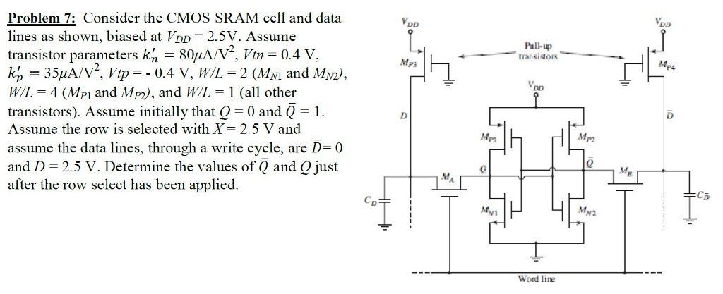
Problem 7: Consider the CMOS SRAM cell and data lines as shown, biased at VDD = 2.5 V. Assume transistor parameters kn′ = 80 μA/V2, V tn = 0.4 V, kp′ = 35 μA/V2, Vtp = −0.4 V, W/L = 2(MN1 and MN2), W/L = 4(MP1 and MP2), and W/L = 1 (all other transistors). Assume initially that Q = 0 and Q¯ = 1. Assume the row is selected with X = 2.5 V and assume the data lines, through a write cycle, are D¯ = 0 and D = 2.5 V. Determine the values of Q¯ and Q just after the row select has been applied.
