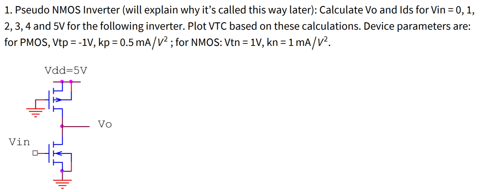
Pseudo NMOS Inverter (will explain why it's called this way later): Calculate Vo and Ids for Vin = 0, 1, 2, 3, 4 and 5 V for the following inverter. Plot VTC based on these calculations. Device parameters are: for PMOS, Vtp = −1 V, kp = 0.5 mA/V2; for NMOS: Vtn = 1 V, kn = 1 mA/V2.
