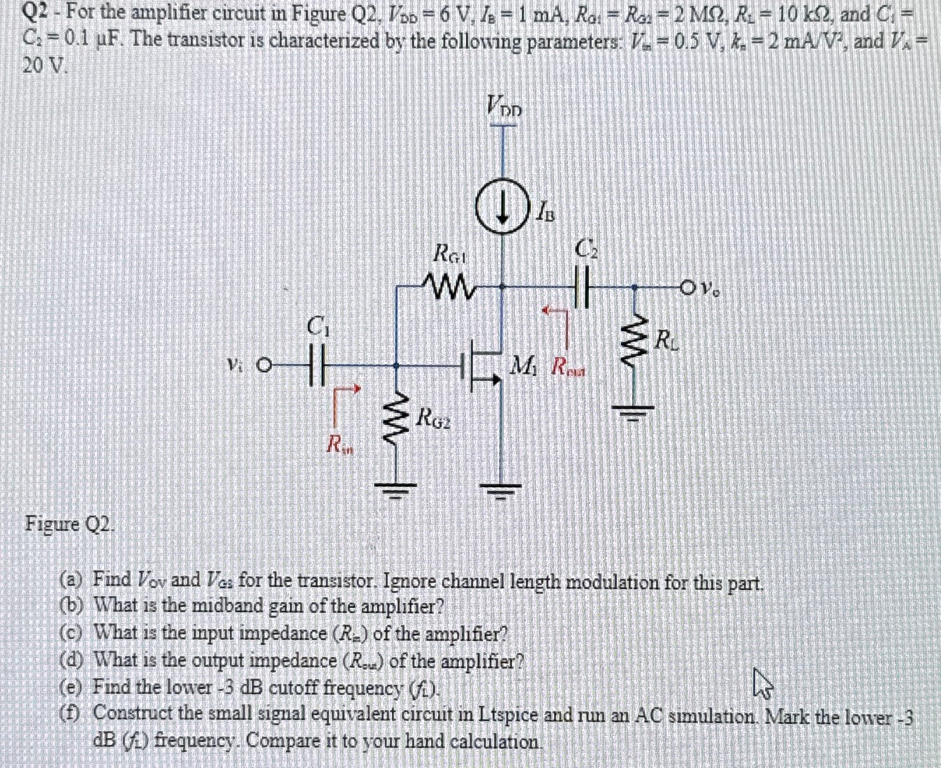
Q2 - For the amplifier circuit in Figure Q2, VDD = 6 V, IB = 1 mA, RG1 = RG2 = 2 MΩ, RL = 10 kΩ, and CA = C2 = 0.1 μF. The transistor is characterized by the following parameters. Vs = 0.5 V, kn = 2 mA/V2, and VA = 20 V Figure Q2. (a) Find Vov and VGs for the transistor. Ignore channel length modulation for this part. (b) What is the midband gain of the amplifier? (c) What is the input impedance (Rm) of the amplifier? (d) What is the output impedance (Ro) of the amplifier? (e) Find the lower −3 dB cutoff frequency (fL). (f) Construct the small signal equivalent circuit in Ltspice and run an AC simulation. Mark the lower -3 dB(f1) frequency. Compare it to your hand calculation.