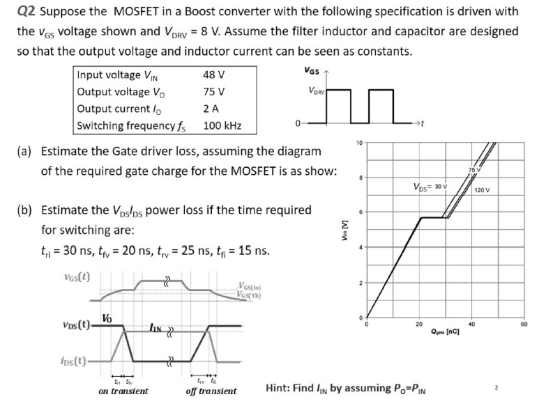
Q2 Suppose the MOSFET in a Boost converter with the following specification is driven with the vGS voltage shown and vDRV = 8 V. Assume the filter inductor and capacitor are designed so that the output voltage and inductor current can be seen as constants. (a) Estimate the Gate driver loss, assuming the diagram of the required gate charge for the MOSFET is as show: (b) Estimate the VDSIDS power loss if the time required for switching are: tri = 30 ns, tfv = 20 ns, trv = 25 ns, tfi = 15 ns. on transient off transient Hint: Find IIN by assuming PO = PIN

![Assume that ID5 = 100 μA, all transistors lengths are 1.2 μm, and CC = 10 pF. For the two-stage op amp shown above, (a) Estimate the -3 dB frequency of the first stage. (10%) (b) Estimate the unit-gain frequency of the opamp. (5%) (c) Find the slew rate. (5%) (d) What circuit changes could be made to double the slew rate but keep unity-gain frequency and CC unchanged? (Assume all channel lengths are fixed) (5%) (e) Follow (d), how should M6 change to maintain zero systematic offset voltage? (54%) (f) Follow (d) and (e), ignoring the body effect, what is the output voltage range of the opamp? What is the range of common-mode input voltage, assuming ±2.5 V power supplies are used? (10%) [Two-Stage CMOS Op Amp + Output Stage] *n-channel MOS transistors: μnCox = 92 μA/V2; Vtn = 0.8 V; ro = 8,000L (μm)/ID(mA) in saturation region * p-channel MOS transistors: μpCox = 30 μA/V2; Vtp = -0.9 V; ro = 12,000L (μm)/ID(mA) in saturation region](https://www.doubtrix.com/js/ckeditor/filemanager/connectors/php/editor/1702192763-Jzmnfiefggzdfvkaf.png)