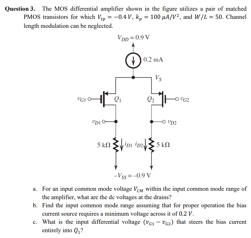
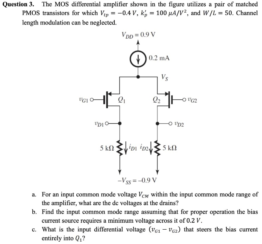
Question 3. The MOS differential amplifier shown in the figure utilizes a pair of matched PMOS transistors for which Vtp = −0.4 V, kp = 100 μA/V2, and W/L = 50. Channel length modulation can be neglected. a. For an input common mode voltage VCM within the input common mode range of the amplifier, what are the dc voltages at the drains? b. Find the input common mode range assuming that for proper operation the bias current source requires a minimum voltage across it of 0.2 V. c. What is the input differential voltage (vG1 − vG2) that steers the bias current entirely into Q1 ?