Vtn = 0.8 V, Vtp = -0.9 V,  = 250
= 250  ,
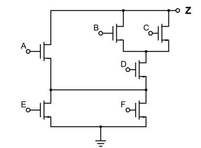
,  =120 is given. The pull-down section of a CMOS logic circuit is shown below.
a) Find the logic expression for Z. What function does this circuit implement?
b) Draw the pull-up network that completes the CMOS logic circuit.
c) Assume that the equivalent inverter has an NMOS transistor with a minimum size of 2 müm/250 nm. Determine the equivalent PMOS transistor dimensions (W/L) that ensure  for the equivalent inverter.
d) Find the NMOS and PMOS transistor dimensions in the CMOS logic circuit so that the propagation delays are equal to the value you found for the inverter in c) for the worst case, assuming an equal load capacitance for both the inverter and the logic circuit.