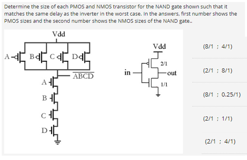
Referring to the figure below, a CMOS gate is shown on the left and the number on each transistor indicates the width of that transistor. We would like to match the worst case delay of the CMOS gate to the inverter delay. Determine the sizes of PMOS and NMOS transistor on the Inverter gate. In the answers, first number shows the PMOS width and the second number shows the NMOS width of the inverter