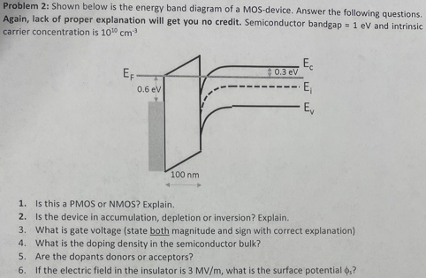
Shown below is the energy band diagram of a MOS-device. Answer the following questions. Again, lack of proper explanation will get you no credit. Semiconductor bandgap = 1 eV and intrinsic carrier concentration is 10^10 cm^-3 1. Is this a PMOS or NMOS? Explain. 2. Is the device in accumulation, depletion or inversion? Explain. 3. What is gate voltage (state both magnitude and sign with correct explanation) 4. What is the doping density in the semiconductor bulk? 5. Are the dopants donors or acceptors? 6. If the electric field in the insulator is 3 MV/m, what is the surface potential φ5?
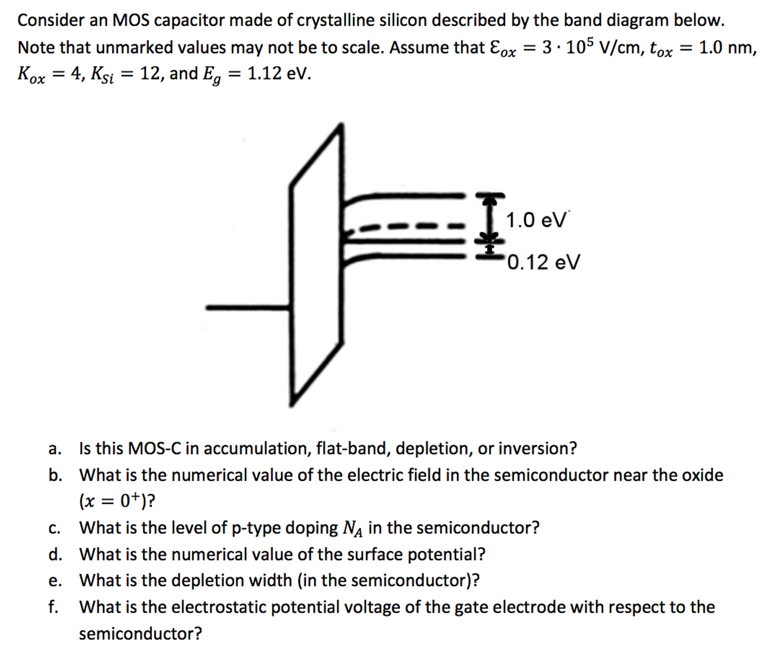
Image text
Shown below is the energy band diagram of a MOS-device. Answer the following questions. Again, lack of proper explanation will get you no credit. Semiconductor bandgap = 1 eV and intrinsic carrier concentration is 10^10 cm^-3 1. Is this a PMOS or NMOS? Explain. 2. Is the device in accumulation, depletion or inversion? Explain. 3. What is gate voltage (state both magnitude and sign with correct explanation) 4. What is the doping density in the semiconductor bulk? 5. Are the dopants donors or acceptors? 6. If the electric field in the insulator is 3 MV/m, what is the surface potential φ5?