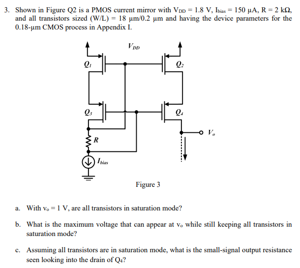
Shown in Figure Q2 is a PMOS current mirror with VDD = 1.8 V, Ibias = 150 μA, R = 2 kΩ, and all transistors sized (W/L) = 18 μm/0.2 μm and having the device parameters for the 0.18−μm CMOS process in Appendix I. Figure 3 a. With vo = 1 V, are all transistors in saturation mode? b. What is the maximum voltage that can appear at vo while still keeping all transistors in saturation mode? c. Assuming all transistors are in saturation mode, what is the small-signal output resistance seen looking into the drain of Q4?