[Small Signal Analysis] Consider the following amplifier circuit consisting of an N-type MOSFET, λ = 0 and vSB = 0. RG = 100kΩ, RD = 3kΩ, RS = 1kΩ, CC and CS are both so large that 1/(jωC) ∼ 0 at the frequency of interest. VDD = 1.0v. The MOSFET has kn = 0.8 mA/V2 and Vt = 0.4v. (a) Analyze the DC bias point of this circuit. What are the DC values of VOUT and VS , respectively? (b) Calculate gm for the MOSFET. (c) What is the maximum allowed value of RD so that the MOS transistor remains in saturation mode? (d) Draw the small signal equivalent circuit for this amplifier. (e) What is the small signal gain Av? (f) What is the input resistance Rin?
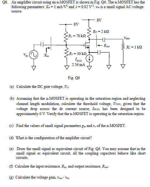
Image text
[Small Signal Analysis] Consider the following amplifier circuit consisting of an N-type MOSFET, λ = 0 and vSB = 0. RG = 100kΩ, RD = 3kΩ, RS = 1kΩ, CC and CS are both so large that 1/(jωC) ∼ 0 at the frequency of interest. VDD = 1.0v. The MOSFET has kn = 0.8 mA/V2 and Vt = 0.4v. (a) Analyze the DC bias point of this circuit. What are the DC values of VOUT and VS , respectively? (b) Calculate gm for the MOSFET. (c) What is the maximum allowed value of RD so that the MOS transistor remains in saturation mode? (d) Draw the small signal equivalent circuit for this amplifier. (e) What is the small signal gain Av? (f) What is the input resistance Rin?
![[Small Signal Analysis] Consider the following amplifier circuit consisting of an N-type MOSFET, λ = 0 and vSB = 0. RG = 100kΩ, RD = 3kΩ, RS = 1kΩ, CC and CS are both so large that 1/(jωC) ∼ 0 at the frequency of interest. VDD = 1.0v. The MOSFET has kn = 0.8 mA/V2 and Vt = 0.4v. (a) Analyze the DC bias point of this circuit. What are the DC values of VOUT and VS , respectively? (b) Calculate gm for the MOSFET. (c) What is the maximum allowed value of RD so that the MOS transistor remains in saturation mode? (d) Draw the small signal equivalent circuit for this amplifier. (e) What is the small signal gain Av? (f) What is the input resistance Rin?](https://www.doubtrix.com/uploads/editor/3805147532ZwJkivSixk.png)

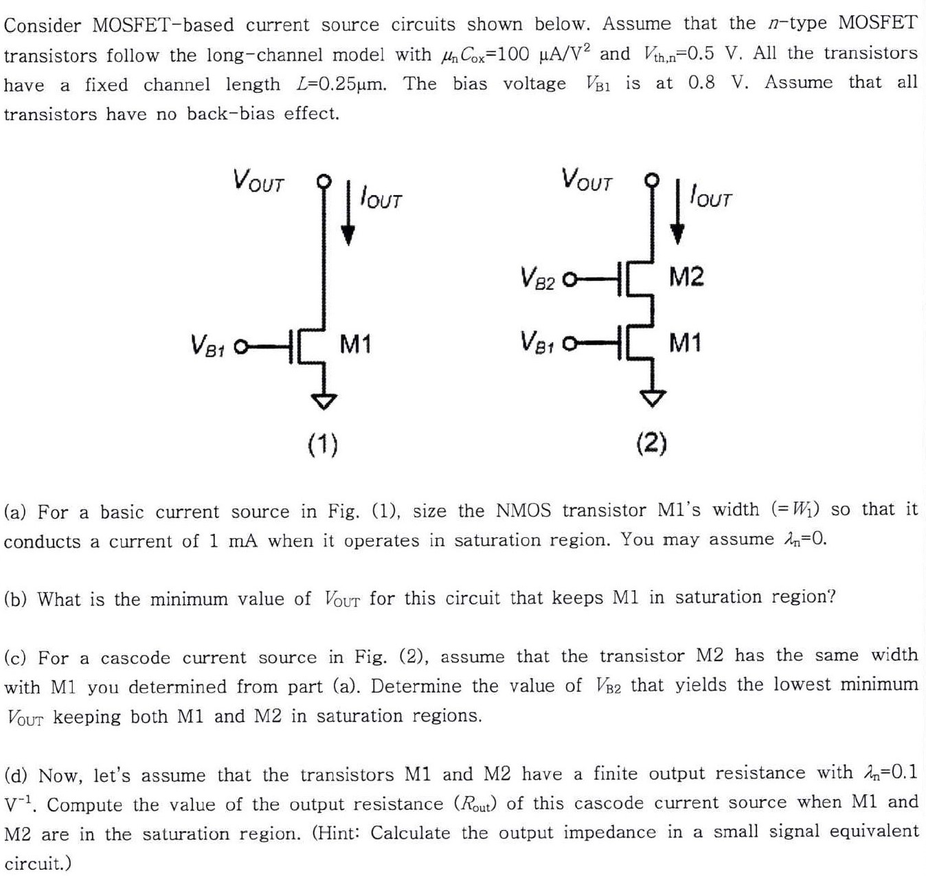
![[MOSFET Circuits] Consider the MOSFET circuit as shown below. R = 1kΩ, kn’ = 1 mA/V2 and Vtn = 0.3 V for both Q1 and Q2, W/L = 0.5μm/0.1μm for Q1, W/L = 1μm/0.1μm for Q2, λ = 0 and vSB = 0. (a) Calculate the voltage at the drain terminal of Q1. (b) What is the ratio of iD1 to iD2, where iD1 is the drain current for Q1 and iD2 is the drain current for Q2. Hint: This circuit is called the "current mirror" circuit, where the ratio of iD1 to iD2 is a fixed number, determined by W1, W2, L1 and L2, as long as both transistors are biased in saturation mode. (c) What is the maximum value of R2 so that Q2 remains in saturation mode?](https://www.doubtrix.com/uploads/editor/0609833589NADbRdqxAb.png)