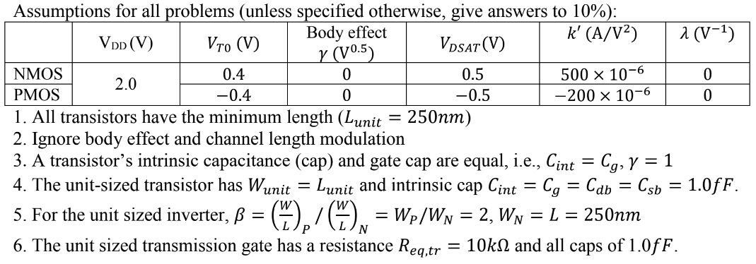
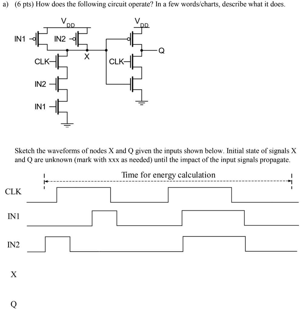
Task 4 Digital Circuits Fig. 4.1 Fig. 4.2 Given are the CMOS gates according to Fig. 4.1 und Fig. 4.2. a) For the gate from Fig. 4.1 determine the output logic values of Y for all possible input logic values A, B, and C and enter them into a truth table. For some logic states you will not be able to determine the output logic value. Denote these states with Y = Z and explain why a definite value for Y cannot be given. b) Now consider the circuit in Fig. 4.2. Determine the output logic values of Y for all possible input logic values A, B, C, and D and enter them into a truth table. c) Draw the circuit diagram of a level-sensitive D-latch and an edge-triggered master-slave Dflipflop. Given is a sequential circuit according to Fig. 4.3. The edge-triggered registers exhibit the following specifications: setup-time tsetup = 200 ps, hold-time thold = 100 ps, propagation delay tpcq = 50 ps, and contamination delay tccq = 50 ps. The maximum clock frequency is 1 GHz. Fig. 4.3 d) Determine the minimal contamination delay tcd for the combinational logic. e) Determine the maximum propagation delay tpd for the combinational logic.