The below diagrams show the pin layout of an early SRAM chipset and the timing diagram. (i) For each CS¯ input pulse at a, b, c, and d, list the mode of operation, the contents of both the Address and the Memory contents. (2 marks) (ii) What is the size of this memory chip? Show your reasoning. (4 marks) (iii) Determine the functions of the Vcc and the GND pins. (2 marks)
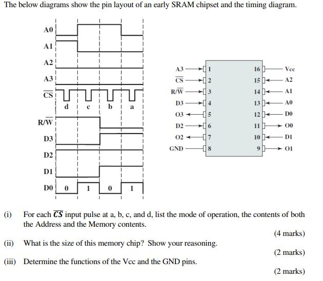
The below diagrams show the pin layout of an early SRAM chipset and the timing diagram. (i) For each CS¯ input pulse at a, b, c, and d, list the mode of operation, the contents of both the Address and the Memory contents. (2 marks) (ii) What is the size of this memory chip? Show your reasoning. (4 marks) (iii) Determine the functions of the Vcc and the GND pins. (2 marks)

Image text
The below diagrams show the pin layout of an early SRAM chipset and the timing diagram. (i) For each C S ¯ input pulse at a, b, c, and d, list the mode of operation, the contents of both the Address and the Memory contents. (ii) What is the size of this memory chip? Show your reasoning. (4 marks) (iii) Determine the functions of the V c c and the GND pins. (2 marks) (2 marks)

Detailed Answer