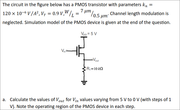
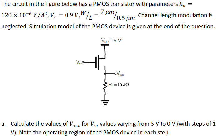
The circuit in the figure below has a PMOS transistor with parameters kn = 120×10−6 V/A2, VT = 0.9 V, W/L = 7 μm/0.5 μm. Channel length modulation is neglected. Simulation model of the PMOS device is given at the end of the question. a. Calculate the values of Vout for Vin values varying from 5 V to 0 V (with steps of 1 V). Note the operating region of the PMOS device in each step.