The circuit of Fig. 4 must be designed for a voltage drop of 100 mV across Rs. Assume the impedance of a capacitor is negligible. Fig. 4 (a) Calculate the minimum allowable value of W/L if M1 must remain in saturation. (10 pt) (b) Based on W/L and VG value calculated in (a), what are the required values of R1 and R2 if the input impedance must be 100 kΩ? (10 pt) Apply for all problems Assume μnCox = 200 μA V2, μpCox = 100 μA V2, VTH = 0.5 for NMOS and −0.5 V for PMOS, λn = λp = 0.01. ro = 1 λID
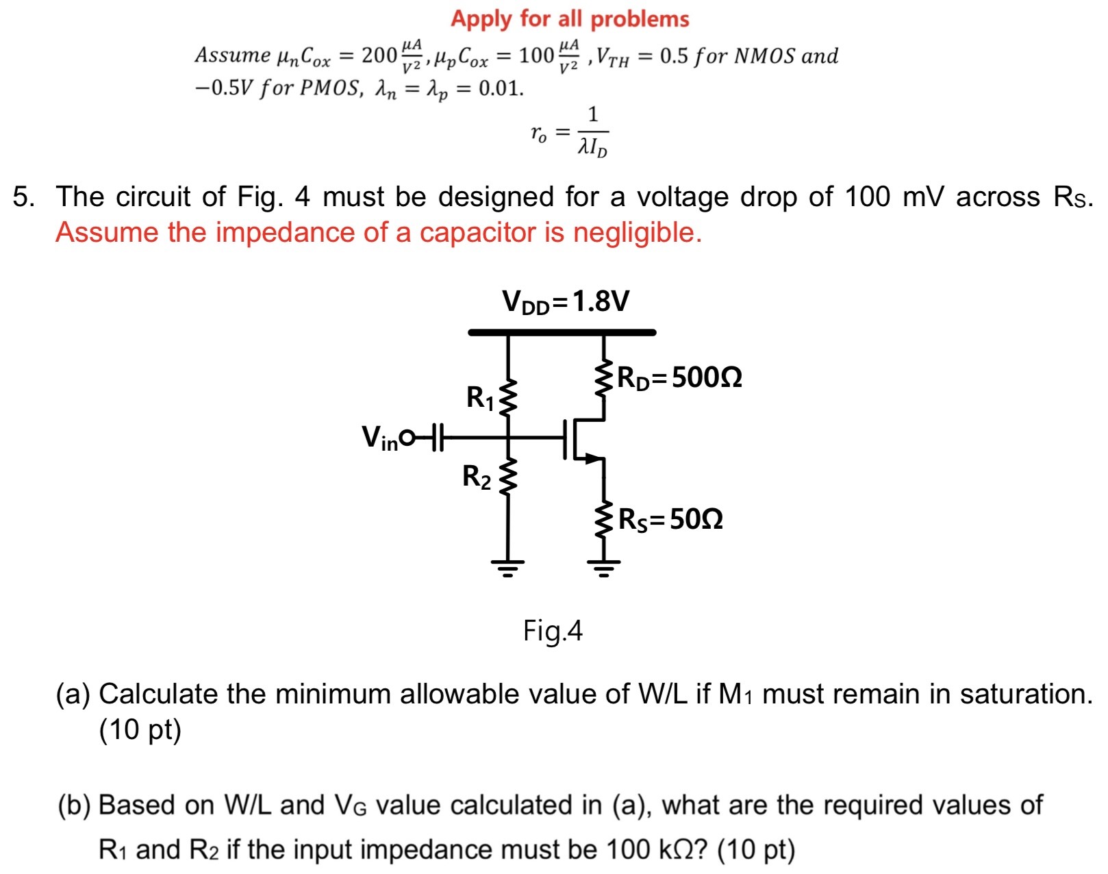
The circuit of Fig. 4 must be designed for a voltage drop of 100 mV across Rs. Assume the impedance of a capacitor is negligible. Fig. 4 (a) Calculate the minimum allowable value of W/L if M1 must remain in saturation. (10 pt) (b) Based on W/L and VG value calculated in (a), what are the required values of R1 and R2 if the input impedance must be 100 kΩ? (10 pt) Apply for all problems Assume μnCox = 200 μA V2, μpCox = 100 μA V2, VTH = 0.5 for NMOS and −0.5 V for PMOS, λn = λp = 0.01. ro = 1 λID

Image text
Apply for all problems Assume μ n C o x = 200 μ A V 2 , μ p C o x = 100 μ A V 2 , V T H = 0.5 for NMOS and 0.5 V for P M O S , λ n = λ p = 0.01 .
r o = 1 λ I D
  1. The circuit of Fig. 4 must be designed for a voltage drop of 100 m V across Rs. Assume the impedance of a capacitor is negligible. Fig. 4 (a) Calculate the minimum allowable value of W / L if M 1 must remain in saturation. (10 pt) (b) Based on W/L and V G value calculated in (a), what are the required values of R 1 and R 2 if the input impedance must be 100 k Ω ? (10 pt)

Detailed Answer