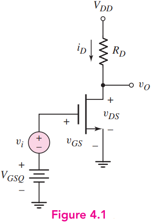
The circuit shown in Figure 4.1 has parameters VDD = 2.5 V and RD = 10 kΩ. The transistor is biased at IDQ = 0.12 mA. The transistor parameters are VTN = 0.3 V, kn’ = 100 μA/V2, and λ = 0. (a) Design the W/L ratio of the transistor such that the small-signal voltage gain is Av = -3.8. (b) Repeat part (a) for Av = -5.0.
Image text
The circuit shown in Figure 4.1 has parameters VDD = 2.5 V and RD = 10 kΩ. The transistor is biased at IDQ = 0.12 mA. The transistor parameters are VTN = 0.3 V, kn’ = 100 μA/V2, and λ = 0. (a) Design the W/L ratio of the transistor such that the small-signal voltage gain is Av = -3.8. (b) Repeat part (a) for Av = -5.0.