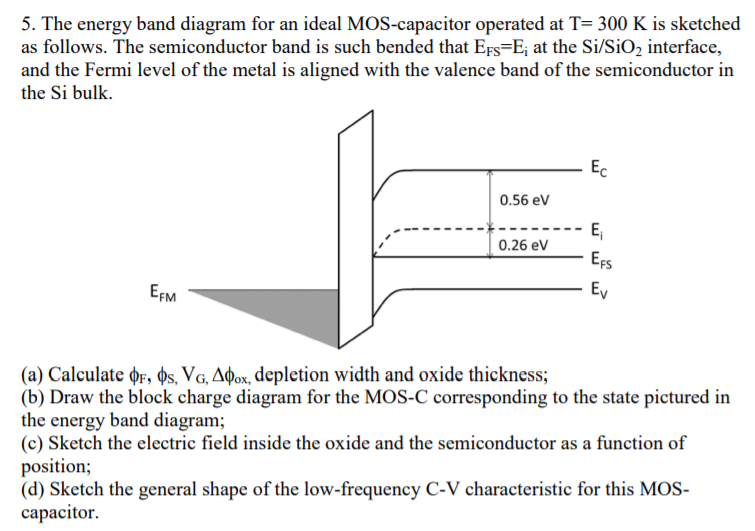
The energy band diagram for an ideal MOS-capacitor operated at T = 300 K is sketched as follows. The semiconductor band is such bended that EFS = Ei at the Si/SiO2 interface, and the Fermi level of the metal is aligned with the valence band of the semiconductor in the Si bulk. (a) Calculate ϕF, ϕs, VG, Δϕox, depletion width and oxide thickness; (b) Draw the block charge diagram for the MOS-C corresponding to the state pictured in the energy band diagram; (c) Sketch the electric field inside the oxide and the semiconductor as a function of position; (d) Sketch the general shape of the low-frequency C-V characteristic for this MOS-capacitor.

![MOS capacitor. The energy band diagram for an MOS capacitor (no charges in the oxide or at the oxide/semiconductor interface) maintained at 300 K is shown below. Note that the slopes of the bands in the oxide are constant. a) (3 pts) For the pictured condition determine the gate bias VG and the operation mode of the MOS capacitor. Explain. b) (3 pts) Sketch on the semi-logarithmic plot the hole concentration [log(p)] inside the semiconductor as a function of x. c) (4 pts) Determine the metal-semiconductor workfunction difference, ΦMS. Explain your steps and sketch the vacuum level. d) (4 pts) Sketch the block charge diagram and the electric field E(x) vs. x.](https://www.doubtrix.com/uploads/editor/3627537192IqKbsqRrJp.jpg)