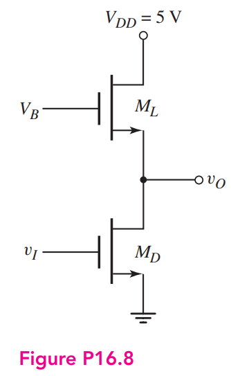
The enhancement-load transistor in the NMOS inverter in Figure P16.8 has a separate bias applied to the gate. Assume transistor parameters of Kn = 1 mA/V2 for MD, Kn = 0.4 mA/V2 for ML, and VTN = 1 V for both transistors. Using the appropriate logic 0 and logic 1 input voltages, determine VOH and VOL for: (a) VB = 4 V, (b) VB = 5 V, (c) VB = 6 V, and (d) VB = 7 V.


You'll get a detailed, step-by-step and expert verified solution.
 Work With Experts to Reach at Correct Answers