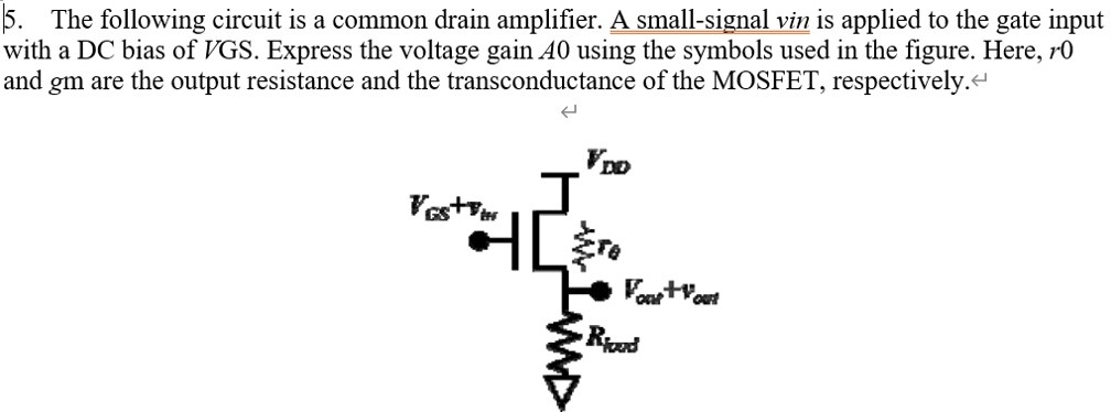
The following circuit is a common drain amplifier. A small-signal vin is applied to the gate input with a DC bias of V GS. Express the voltage gain A0 using the symbols used in the figure. Here, r0 and gm are the output resistance and the transconductance of the MOSFET, respectively.
The following circuit is a common drain amplifier. A small-signal vin is applied to the gate input with a DC bias of V GS. Express the voltage gain A0 using the symbols used in the figure. Here, r0 and gm are the output resistance and the transconductance of the MOSFET, respectively.

Image text
  1. The following circuit is a common drain amplifier. A small-signal vin is applied to the gate input with a DC bias of V GS. Express the voltage gain A 0 using the symbols used in the figure. Here, r 0 and g m are the output resistance and the transconductance of the MOSFET, respectively.

Detailed Answer