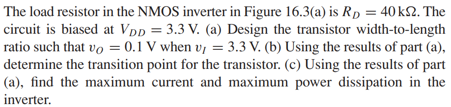
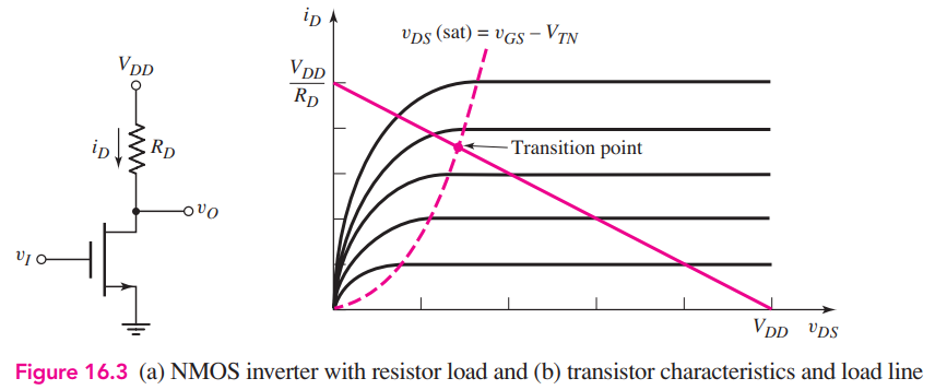
The load resistor in the NMOS inverter in Figure 16.3(a) is RD = 40 kΩ. The circuit is biased at VDD = 3.3 V. (a) Design the transistor width-to-length ratio such that vO = 0.1 V when vI = 3.3 V. (b) Using the results of part (a), determine the transition point for the transistor. (c) Using the results of part (a), find the maximum current and maximum power dissipation in the inverter.

You'll get a detailed, step-by-step and expert verified solution.
 Work With Experts to Reach at Correct Answers