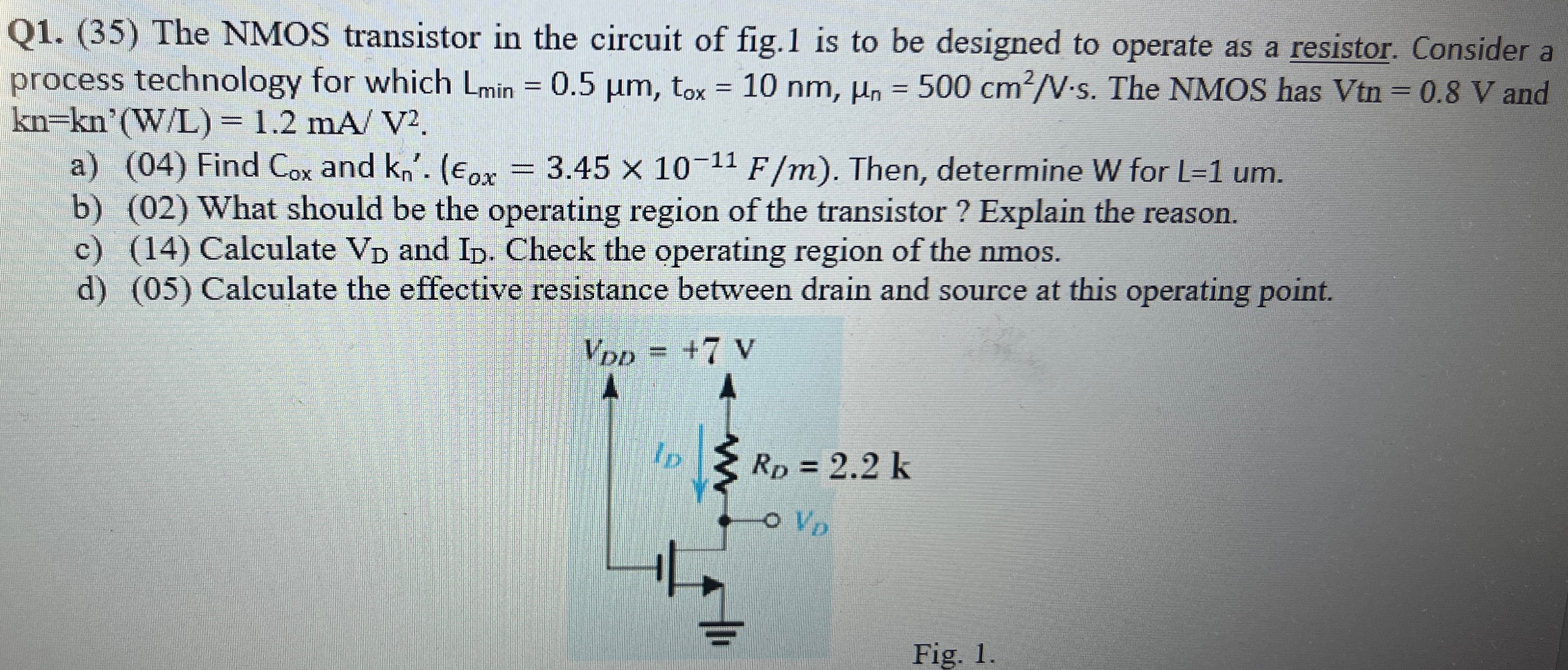
The NMOS transistor in the circuit of fig. 1 is to be designed to operate as a resistor. Consider a process technology for which Lmin = 0.5 μm, tox = 10 nm, μn = 500 cm2 /V⋅s. The NMOS has Vtn = 0.8 V and kn = kn′(W/L) = 1.2 mA/V2. a) (04) Find Cox and kn. (ϵox = 3.45×10⁻¹¹ F/m). Then, determine W for L = 1 um. b) (02) What should be the operating region of the transistor? Explain the reason. c) (14) Calculate VD and ID. Check the operating region of the nmos. d) (05) Calculate the effective resistance between drain and source at this operating point. Fig. 1.