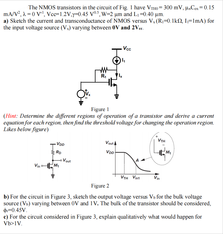
The NMOS transistors in the circuit of Fig. 1 have VTH0 = 300 mV, unCox = 0.15 mA/V2, lambda = 0 V-1, Vcc = 1.2 V, gamma = 0.45 V0.5, W = 2 um and L1 = 0.40 um. a) Sketch the current and transconductance of NMOS versus Vx(R1=0.1kohm, I1=1 mA) for the input voltage source (Vx) varying between 0V and 2Vcc. (Hint: Determine the different regions of operation of a transistor and derive a current equation for each region, then find the threshold voltage for changing the operation region. Likes below figure) b) For the circuit in Figure 3, sketch the output voltage versus Vb for the bulk voltage source (Vb) varying between 0 V and 1 V. The bulk of the transistor should be considered, phiF = 0.45 V. c) For the circuit considered in Figure 3, explain qualitatively what would happen for Vb > 1 V.

You'll get a detailed, step-by-step and expert verified solution.
 Work With Experts to Reach at Correct Answers
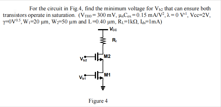
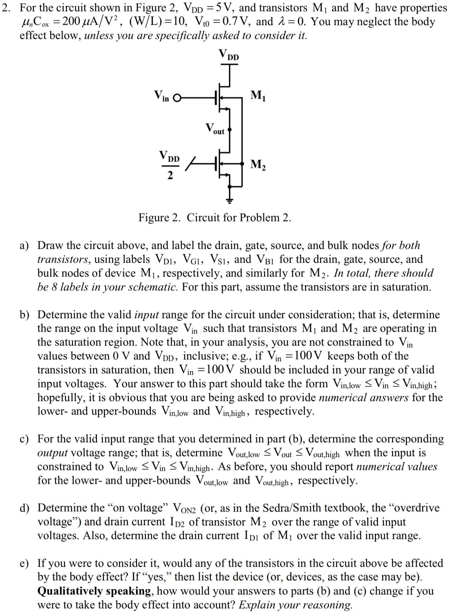
![(a) Figure Q2(a) shows a differential amplifier with a current source at the bottom. It is given that VDD = VSS = 15 V, ISS = 300 μA, Early effect can be ignored (λ = 0), Kn = 400 μA/V2 and VTN = 1 V. You may assume MOSFET in saturation region. (i) For single ended outputs, draw the half-circuits and derive the algebraic equations for the differential mode and common-mode gains as well as CMRR. [6 Marks] (ii) For the above case of single ended output, what should be the value of Rss to get CMRR = 100? [4 Marks] Figure Q2(a) (b) Figure Q2(b) shows a MOSFET based current mirror. Draw the AC small signal model and derive an equation for output resistance Rout as shown in the figure. You can keep your answer in terms of gm, ro etc but denote the subscript 1,2,3 etc to indicate which transistor. In other words, denote transconductance of M2 by writing gm2 and so on. [6 marks] (c) Draw the diagram of a BJT based Class B push-pull power amplifier and derive the maximum possible power efficiency of this circuit. You may ignore crossover distortion and assume |VCE(sat)| = 0 V. [9 marks]](https://www.doubtrix.com/uploads/editor/1710360410ITbaKcVzzE.jpg)