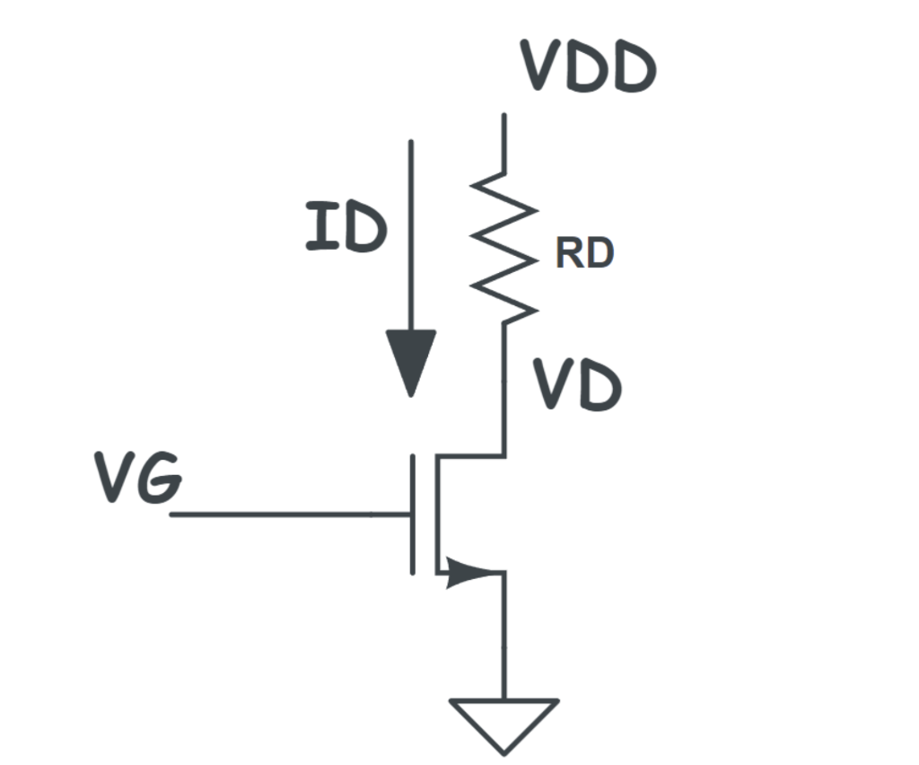
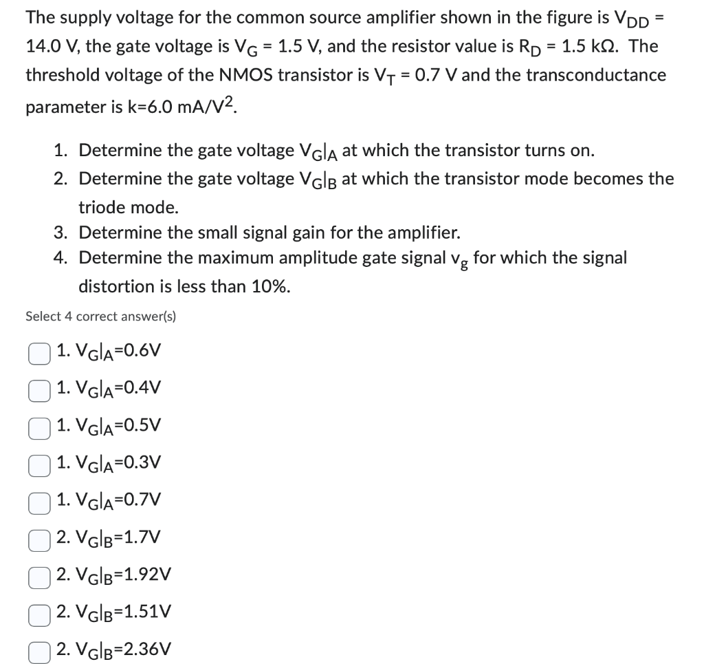
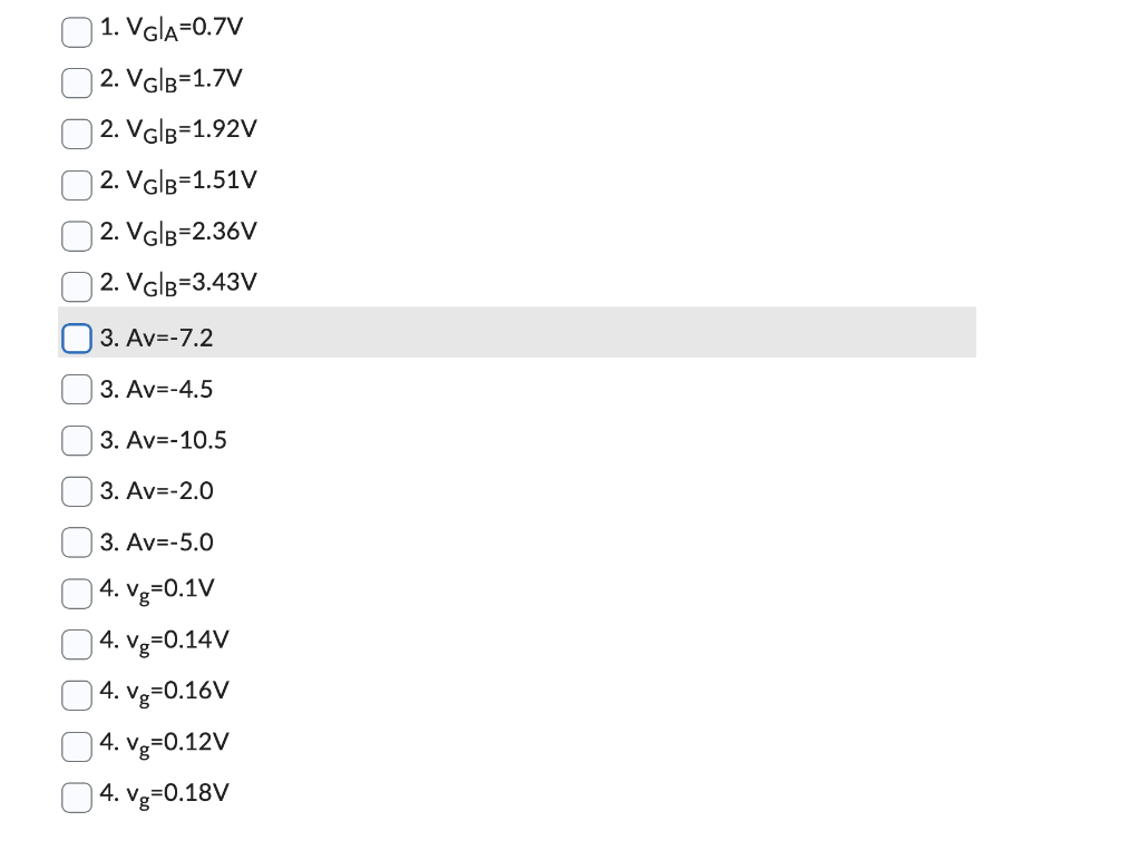
The supply voltage for the common source amplifier shown in the figure is VDD = 14.0 V, the gate voltage is VG = 1.5 V, and the resistor value is RD = 1.5 kohm. The threshold voltage of the NMOS transistor is VT = 0.7 V and the transconductance parameter is k = 6.0 mA/V^2. 1. Determine the gate voltage VG |A at which the transistor turns on. 2. Determine the gate voltage VG|B at which the transistor mode becomes the triode mode. 3. Determine the small signal gain for the amplifier. 4. Determine the maximum amplitude gate signal vg for which the signal distortion is less than 10%.
Image text
The supply voltage for the common source amplifier shown in the figure is VDD = 14.0 V, the gate voltage is VG = 1.5 V, and the resistor value is RD = 1.5 kohm. The threshold voltage of the NMOS transistor is VT = 0.7 V and the transconductance parameter is k = 6.0 mA/V^2. 1. Determine the gate voltage VG |A at which the transistor turns on. 2. Determine the gate voltage VG|B at which the transistor mode becomes the triode mode. 3. Determine the small signal gain for the amplifier. 4. Determine the maximum amplitude gate signal vg for which the signal distortion is less than 10%.