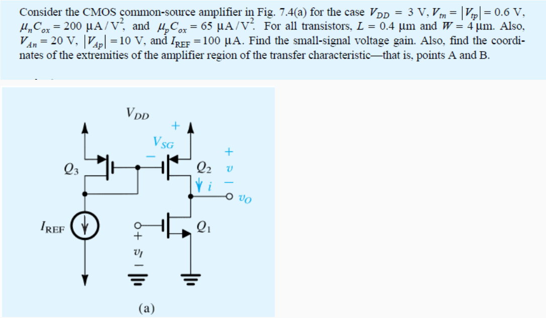
VI. Draw the small signal model, including source-drain resistance, and find the small-signal gain (in V/V) for this current-mirror loaded CS transistor amplifier. For all transistors: W/L = 50 Vt = |0.5 V| VA = 20 V IREF = 100 µA µnCox = 100 µA/V^2 µpCox = 50 µA/V^2 iD = 1/2µnCoxW/L(VOV )^2 gm = µnCoxW/L VOV = 2ID/Vov = √2µnCoxW/LID
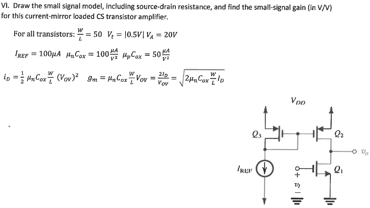
The given circuit is a common-source amplifier with active load as current-mirror formed by PMOS transistors Q2 and Q3. NMOS Q1 is a driver transistor. Input signal is applied at gate terminal of driver transistor. By default, all transistors are assumed to bias in saturaton region. Use following steps to determine voltage gain of the given amplifier circuit.
Step (1): Determine drain current of NMOS Q1/Q2 transistor.
Step (2): Transconductance gm1 of NMOS transistor, Q1.
Step (3): Output resistance ro1 & ro2 of NMOS transistor Q1 & Q2 respectively.
Step (4): Draw small-signal model of the amplifier circuit. Use transconductance and output resistances to calculate small-signal voltage gain, Av.

You'll get a detailed, step-by-step and expert verified solution.
 Work With Experts to Reach at Correct Answers