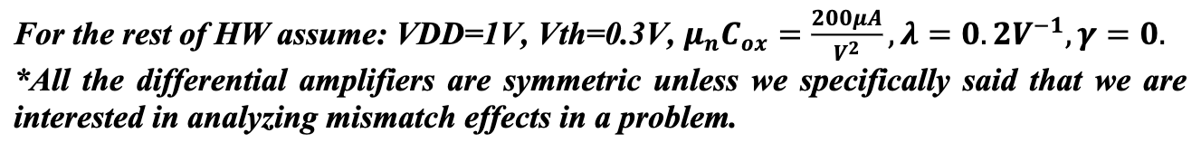
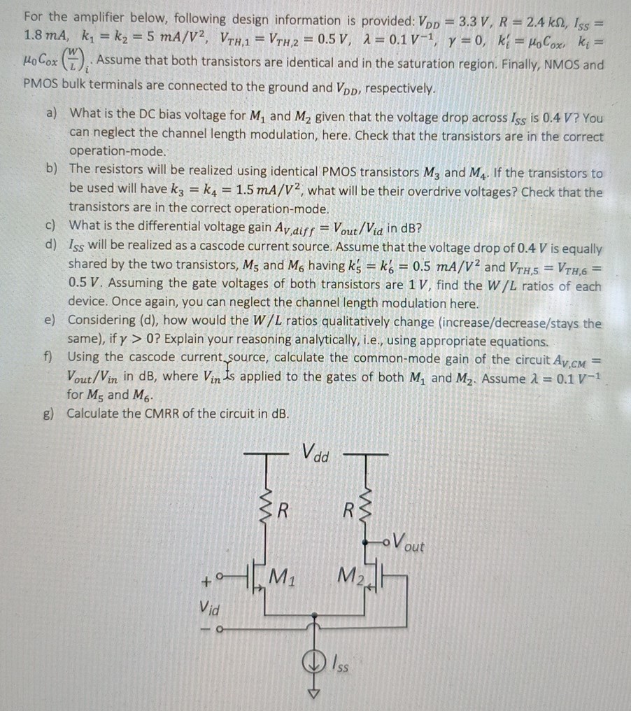
We can make a differential pair amplifier with PMOS input devices as shown below. Suppose circuits are completely symmetric (RDS are equal, M1,2 are similar, and each tail current source requires minimum of Vod to operate) a) What is the single-ended and differential output swing? b) Draw DM and CM half-circuits. (assume that the tail current source has an output impendence of RSS) c) Calculate DM and CM gains. d) What is the acceptable input CM range? e) Compare the results from (d) with the NMOS diff pair we studied in the class. For the rest of HW assume: VDD = 1 V, Vth = 0.3 V, μnCox = 200 μAV2, λ = 0.2 V−1, γ = 0. *All the differential amplifiers are symmetric unless we specifically said that we are interested in analyzing mismatch effects in a problem.