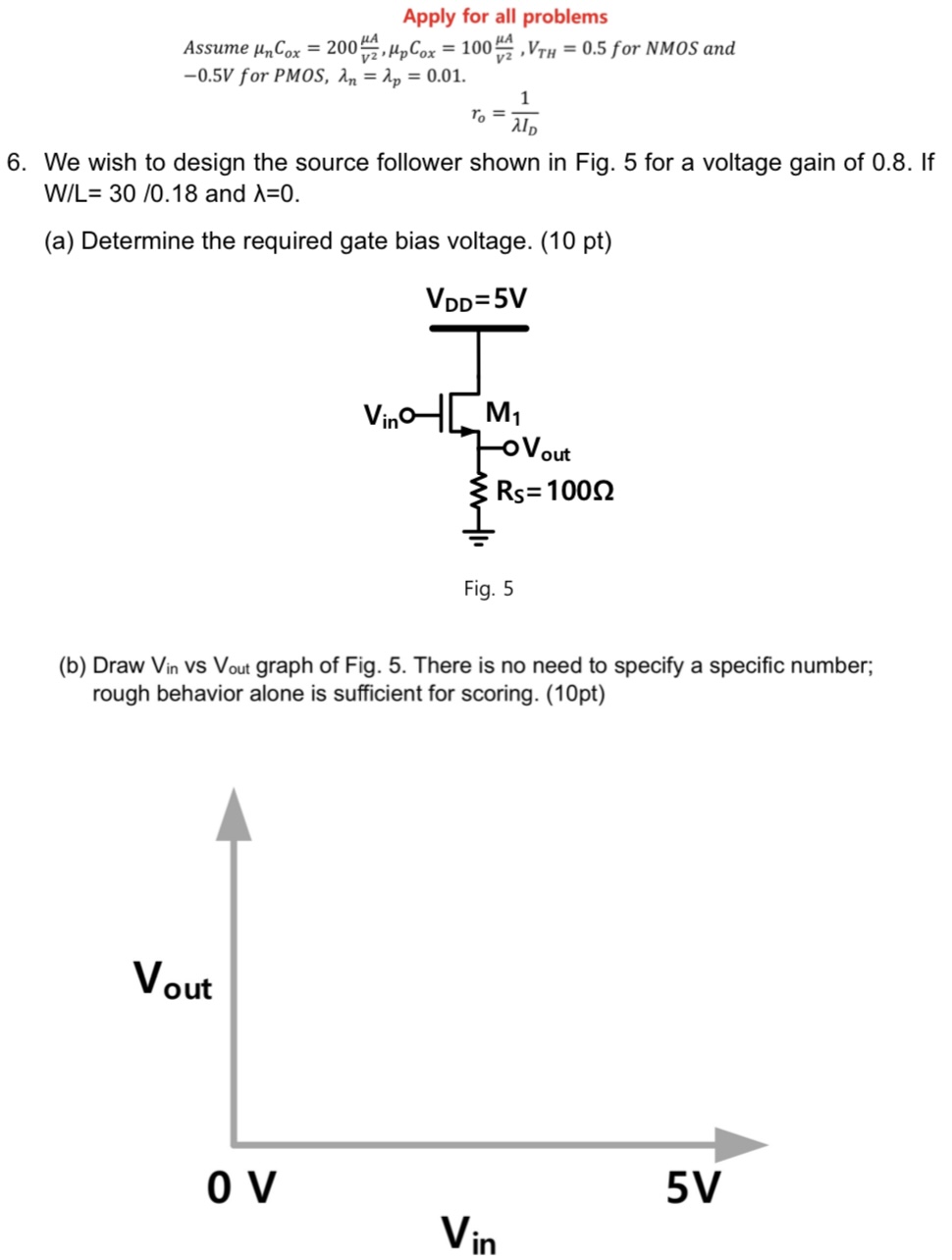
We wish to design the source follower shown in Fig. 5 for a voltage gain of 0.8 . If W/L = 30/0.18 and λ = 0. (a) Determine the required gate bias voltage. (10 pt) Fig. 5 (b) Draw Vin vs Vout graph of Fig. 5 . There is no need to specify a specific number; rough behavior alone is sufficient for scoring. (10 pt) Apply for all problems Assume μnCox = 200 μA V2, μpCox = 100 μA V2, VTH = 0.5 for NMOS and −0.5 V for PMOS, λn = λp = 0.01. ro = 1 λID
We wish to design the source follower shown in Fig. 5 for a voltage gain of 0.8 . If W/L = 30/0.18 and λ = 0. (a) Determine the required gate bias voltage. (10 pt) Fig. 5 (b) Draw Vin vs Vout graph of Fig. 5 . There is no need to specify a specific number; rough behavior alone is sufficient for scoring. (10 pt) Apply for all problems Assume μnCox = 200 μA V2, μpCox = 100 μA V2, VTH = 0.5 for NMOS and −0.5 V for PMOS, λn = λp = 0.01. ro = 1 λID

Image text
Apply for all problems Assume μ n C o x = 200 μ A V 2 , μ p C o x = 100 μ A V 2 , V T H = 0.5 for NMOS and 0.5 V for P M O S , λ n = λ p = 0.01 .
r o = 1 λ I D
  1. We wish to design the source follower shown in Fig. 5 for a voltage gain of 0.8 . If W / L = 30 / 0.18 and λ = 0 . (a) Determine the required gate bias voltage. (10 pt) Fig. 5 (b) Draw V in vs V out graph of Fig. 5 . There is no need to specify a specific number; rough behavior alone is sufficient for scoring. (10pt)

Detailed Answer