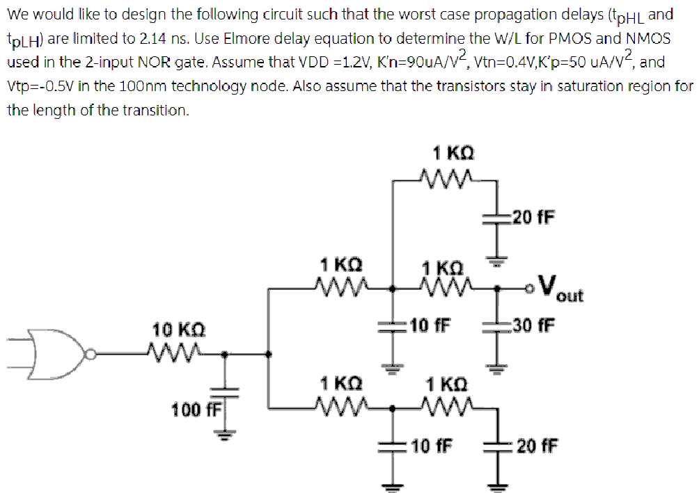
We would like to design the following circuit such that the worst case propagation delays (tpHL and tpLH ) are limited to 2.14 ns. Use Elmore delay equation to determine the W/L for PMOS and NMOS used in the 2 -input NOR gate. Assume that VDD = 1.2 V, K′n = 90 uA/V2, Vtn = 0.4 V, K′p = 50 uA/V2, and Vtp = −0.5 V in the 100 nm technology node. Also assume that the transistors stay in saturation region for the length of the transition.