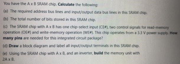
You have the A x B SRAM chip. Calculate the following: (a) The required address bus lines and input/output data bus lines in this SRAM chip. (b) The total number of bits stored in this SRAM chip. (c) The SRAM chip with A×B has one chip-select input (CE#), two control signals for read-memory operation (OE#) and write-memory operation (WE#). This chip operates from a 3.3 V power supply. How many pins are needed for this integrated circuit package? (d) Draw a block diagram and label all input/output terminals in this SRAM chip. (e) Using the SRAM chip with A×B, and an inverter, build the memory unit with 2 A×B.
